
W1 square strip silicon detector from Micron Semiconductor Limited. Active dimensions: 49.50 x 49.50 mm. Explore catalogue variants, packaging and thickness options. Request a detailed datasheet or quotation.
W1 — design specifications
Explore our range of silicon detector designs using the search and filters below. Search by detector type, active dimensions, geometry, strip count and package, then select a design to view its specifications and available options.
Our catalogue is a starting point, not the limit of what we can offer. We can adapt existing designs or develop a new detector to match your requirements.
If you cannot find a suitable design, or would like help choosing a detector, contact our design and sales team at sales@micronsemiconductor.co.uk to discuss your application.
3 catalogue variants
No matching variants. Try widening the size range or clearing a filter.
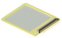 Strip · SquareW149.50 x 49.50 mmStandard FR4.Thickness: Below 20 umSingle sided
Junction strips / rings / sectors: 16
Junction pitch (as listed): 3100
Ohmic strips / rings / sectors: Not applicable
Ohmic pitch (as listed): Not applicable
View design details
- Active dimensions (mm)
- 49.50 x 49.50
- Chip dimensions (mm)
- 54.60 x 54.60
- Readout
- Single sided
- Junction segmentation / array
- 16
- Ohmic segmentation / array
- Not applicable
- Junction pitch (µm unless angular)
- 3100
- Ohmic pitch (µm unless angular)
- Not applicable
- Listed thickness range (µm)
- Below 20 um
- Junction window / implant types
- 2/79/9,5
- Junction metallisation codes
- M
- Ohmic window / implant types
- 2
- Ohmic metallisation codes
- M
- Package options
- Standard FR4.
- Wafer size (inch; footnotes retained)
- 6
Catalogue ß marker: thicknesses of 50 µm or below not requiring NRE; confirm the applicable variant.
Catalogue page 32 · Variant msl-0178. Assembly images illustrate the listed design; final assembly is confirmed with your quotation.
View original catalogue row ↗Detailed IV curves, alpha response and device-specific characterisation are available on enquiry. Listed ranges do not guarantee every thickness, window and package combination.
Request datasheet / quotation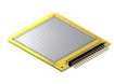 Strip · SquareW149.50 x 49.50 mmRange of designs in different materials.Thickness: Below 50 um 50 – 1500 um 65 – 1500 umSingle or double sided (catalogue: Double sided)
Junction strips / rings / sectors: 16
Junction pitch (as listed): 3100
Ohmic strips / rings / sectors: 16
Ohmic pitch (as listed): 3100
View design details
- Active dimensions (mm)
- 49.50 x 49.50
- Chip dimensions (mm)
- 53.78 x 53.78
- Readout
- Double sided
- Junction segmentation / array
- 16
- Ohmic segmentation / array
- 16
- Junction pitch (µm unless angular)
- 3100
- Ohmic pitch (µm unless angular)
- 3100
- Listed thickness range (µm)
- Below 50 um 50 – 1500 um 65 – 1500 um
- Junction window / implant types
- 2/79/9,5
- Junction metallisation codes
- M/G/P/T
- Ohmic window / implant types
- 2
- Ohmic metallisation codes
- M
- Package options
- Range of designs in different materials.
- Wafer size (inch; footnotes retained)
- 4
Catalogue ß marker: thicknesses of 50 µm or below not requiring NRE; confirm the applicable variant.
Catalogue page 35 · Variant msl-0195. Assembly images illustrate the listed design; final assembly is confirmed with your quotation.
View original catalogue row ↗This catalogue entry describes the double-sided design. A single-sided configuration is also available; please confirm the required segmentation, pitch and contacts with our design and sales team.
Detailed IV curves, alpha response and device-specific characterisation are available on enquiry. Listed ranges do not guarantee every thickness, window and package combination.
Request datasheet / quotation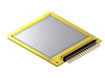 Strip · SquareW149.50 x 49.50 mmRange of designs in different materials.Thickness: 140 – 1500 umSingle or double sided (catalogue: Double sided)
Junction strips / rings / sectors: 16
Junction pitch (as listed): 3100
Ohmic strips / rings / sectors: 16
Ohmic pitch (as listed): 3100
View design details
- Active dimensions (mm)
- 49.50 x 49.50
- Chip dimensions (mm)
- 54.60 x 54.60
- Readout
- Double sided
- Junction segmentation / array
- 16
- Ohmic segmentation / array
- 16
- Junction pitch (µm unless angular)
- 3100
- Ohmic pitch (µm unless angular)
- 3100
- Listed thickness range (µm)
- 140 – 1500 um
- Junction window / implant types
- 2/79/9,5
- Junction metallisation codes
- M/G
- Ohmic window / implant types
- 2
- Ohmic metallisation codes
- M
- Package options
- Range of designs in different materials.
- Wafer size (inch; footnotes retained)
- 6
Catalogue page 35 · Variant msl-0196. Assembly images illustrate the listed design; final assembly is confirmed with your quotation.
View original catalogue row ↗This catalogue entry describes the double-sided design. A single-sided configuration is also available; please confirm the required segmentation, pitch and contacts with our design and sales team.
Detailed IV curves, alpha response and device-specific characterisation are available on enquiry. Listed ranges do not guarantee every thickness, window and package combination.
Request datasheet / quotationUnderstanding the options
Window numbers identify implant / entrance-window types. Metallisation codes describe coverage: M continuous, G grid, P periphery, T thin coverage with periphery, DM double metal and E equipotential bands. Ask us to confirm the best combination for your particle type, energy, electronics and environment.
Catalogue ranges are design options rather than stock listings. Published information supports initial selection; Micron confirms the final specification, availability and application suitability.